
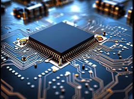
An Explanation of Common PCB Failure Modes
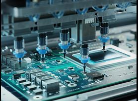
PCB manufacturers rely on product monitoring and testing to check their products’ functionality and compliance, but with industry pressures driving continuous innovation, product failures inevitably happen. Though manufacturers may have sophisticated screening techniques and use good manufacturing practices, modern PCBs are especially complex, and greater complexity leads to more possible failure modes than ever before.
Common PCB failure modes
On top of rapid innovation, shrinking components, and sophisticated circuit geometries, the fabrication of a printed circuit board consists of many steps and moving parts. The nature of the manufacturing process creates numerous opportunities to unintentionally introduce a defect. Failure analysts have noted several processes and tendencies that are more likely to be associated with PCB failure:
High-speed printed circuit boards (HSCBs)
HSCBs, which have grown more complex and use a variety of integrated components, continue to grow in popularity. However, the components require boards that are composed of two or three materials that increase the possibility of failure in extremely high-speed applications. Failures also occur from pins and chips placed in an incorrect manner on the board.
Lead-free assembly processes
The lead-free assembly process requires a higher temperature than traditional lead solder, which leads to higher temperatures for the reflow and wave soldering. This results in an adverse effect on the solder joint and electronic components. Tin solder also has a propensity to spontaneously form “tin whiskers” which can cause electrical shorts.
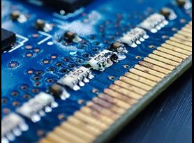
Plated through hole barrel cracking
Barrel fatigue, which is the circumferential cracking of the copper plating that forms the plated through hole (PTH wall), is the most prevalent failure mode. It occurs as a result of differential expansion between the copper plating and the out-of-plane coefficient of thermal expansion (CTE) of the printed board.
Surface finish selection
The most important decision for the electronic assembly may be the surface furnish, which affects the process yield, the amount of rework necessary, field failure rate, the ability to test, the scrap rate, and the cost.
Conductive anodic filaments
Conductive Anodic Filaments (CAF) or metallic electro-migration describes an electro-chemical process that involves the transport of a metal across a nonmetallic medium under the influence of an applied electric field. The condition causes current leakage, intermittent electrical shorts, and dielectric breakdown between conductors in PCBs.
These are just a few of the many failure modes associated with PCBs, and all must be considered carefully when assessing a product and its manufacturing process. Prevention is always the best strategy, but when a product does fail – whether during testing or in use – root cause analysis provides manufacturers with a tool that can bolster PCB fabrication processes, improve identification of failure characteristics, troubleshoot, and improve overall efficiency.
If you have questions about failure analysis or the root causes of failure for PCBs, contact the experts at Element. Our testing professionals have decades of experience testing and providing failure analysis for PCBs and other electronic components. We are happy to provide information about our services and capabilities or simply answer your preliminary questions.
Find related Resources
Learn more
Printed Circuit Board Testing
Ensure your printed circuit boards and finished printed circuit assemblies are of the highest quality and compliant with relevant standards with comprehensive PCB testing from Element.
Conductive Anodic Filament (CAF) Testing
Element’s comprehensive PCB testing includes industry-leading conductive anodic filament (CAF) testing to IPC-TM-650 and to your specific requirements.
Tin Whisker Testing
Find the right strategy to prevent tin whisker growth in your electronic components with testing support from Element.
Printed Circuit Board (PCB) Failure Analysis
Understand and rectify the root causes of PCB failure with industry-leading PCB failure analysis from the testing experts at Element.