Why perform cross-sectional examination of circuit boards?
In this article, Element's experts reveal why cross-sectional analysis is critical for PCB reliability, exposing hidden defects that visual and X-ray inspection miss. This metallographic technique uncovers microcracks in solder joints, voids in BGAs, and intermetallic formation - even in boards that pass thermal cycling tests - providing manufacturers essential insights to prevent catastrophic field failures.
The integrity of circuit boards cannot always be ensured by non-destructive techniques, such as visual and X-ray inspection means. Cross-sectional examination at high magnification may also be required.
Cross-sectioning (sometimes called micro-sectioning) is a metallographic technique used to characterize materials, perform a failure analysis, and expose an internal structure of a printed circuit board (PCB) or an electronic component package. Cross-sectioning involves mounting a target segment of the PCB in a potting material to obtain support and protect the sample in the subsequent polishing process. The mounted sample is carefully polished using progressively finer media to reach the target examination plane of interest. The prepared specimen is then examined at various magnifications either under an optical microscope or scanning electron microscopy (SEM). This process is defined by the IPC TM-650 2.1.1 procedure. The equipment list below showcases some of the major equipment used in the cross-sectioning sample preparation and analysis:
- A polishing machine is used to prepare the surface of the target component for evaluation, where polishing papers with different grits are used at different stages of the polishing process. Normally progressively finer grits are used in the polishing process, with silica or alumina powders of 0.05 micrometer as the final polishing step.
- An optical microscope called a “metallograph” is used to examine the microstructure of a cross-sectioned specimen at various magnifications up to 1000x magnification, with limited depth of field. Mounted specimens can be observed either in the as-polished or etched conditions.
- A scanning electron microscope (SEM) is used to examine board surfaces or cross-sectional samples. Due to its high depth of field, specimens do not have to be polished for SEM examination. The SEM can operate under various modes, such as secondary electron (SE) mode or backscattered electron mode (BSE) at either high vacuum or variable pressure (to accommodate nonconductive samples). SE mode provides topographic information on the sample surface; BSE mode can be used for topography as well as elemental contrast at various magnifications from 10 to 200,000x magnification. The SEM is also capable of energy dispersive spectroscopy (EDS), which can provide direct qualitative and semi-quantitative element analysis on a localized spot of the specimen.
Although destructive in nature, the cross-sectional examination can reveal invaluable detail of the internal PCB structure, which the non-destructive visual or x-ray inspection is unable to provide [1,2]. For example, cross-sectional examination reveals the solder grain structure, intermetallic boundary conditions between the solder and a conductor pad, cracks and voids, and even the composition of a tiny inclusion. A study of these details helps to quickly determine the root cause of a failure. In addition, the measurements of the internal structure such as the copper plating thickness and intermetallic boundary thickness can be performed, which is useful information for process control or checks. Figures 1 through 3 present some examples of typical PCB cross-sections.
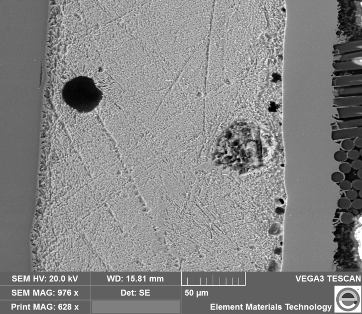
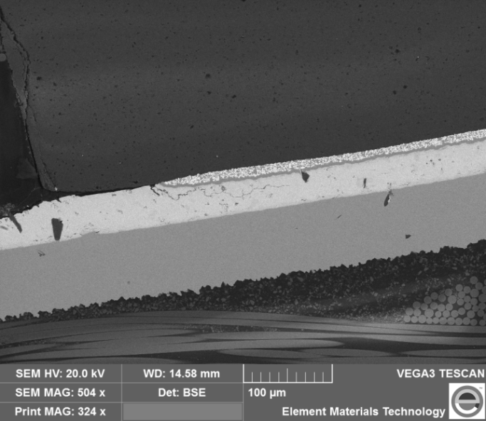
Figure 3. A cross-sectioned and plated-through hole observed via SEM. The view shows the copper terminal (on the left), the copper-plated wall of the hole, glass fibers (on the right), and voids of various sizes in the solder joint. OM=976X.
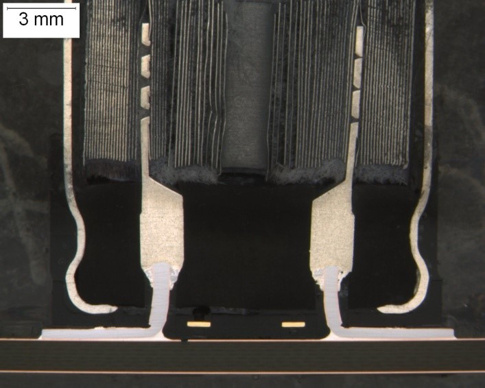
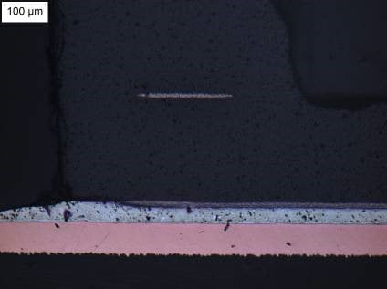
Figure 1. A cross-sectioned electrolytic capacitor with the internal structure exposed. The structure consists of an aluminum housing, wound anode and cathode aluminum foils, and inner aluminum terminals welded to iron outer terminals. The outer terminals are copper-plated and soldered to the PCB. Original Magnification (OM) = 5X.
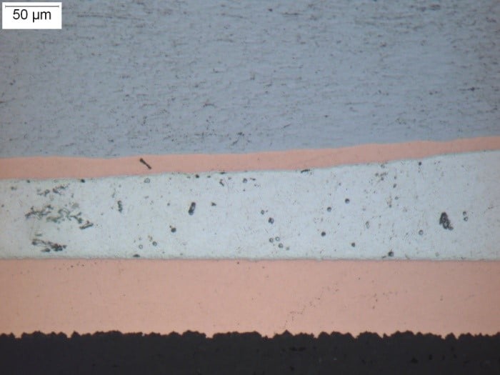
Figure 2a. One of the solder joints of the capacitor is shown at higher magnification. OM=50X.
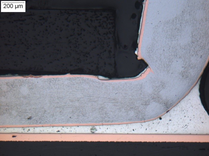
Figure 2b. One of the solder joints of the capacitor is shown at higher magnification 200X.
Cross-section analysis can be conducted at different stages of PCB production. It is a conventional test for plated through-hole or via evaluation, as well as the examination of dielectric lamination conditions, inner layer copper thickness and trace width in the laminated board production. Cross-section analysis is also a critical test for the assembled PCBAs. Only this analysis can check for :
-
Voids or cracks
-
Ball grid array (BGAs), to see if the solder joints are formed properly
-
The amount of solder build-up, through-hole filling, wetting conditions, and voids in solder joints
-
Grain coarsening, intermetallic formation, and tin whisker growth after thermal cycling
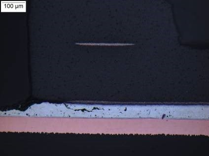
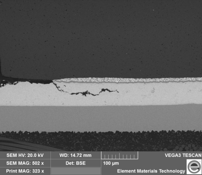
In particular, cross-section analysis is conducted when a failure occurs. Sometimes, the cross-section inspection had been skipped for the parts that passed the thermal cycling test visually; however, Element has found that it is critical to evaluate solder joint conditions, even when parts have passed the cycling tests, as microracks can form in the solder joints that are often undetected in non-destructive evaluations.. The post-test cross-sectional analysis provides valuable information, such as how much damage the test has caused on the components and solder joints, and in what forms the damage has taken. As a result, the PCB reliability can be assessed more accurately.
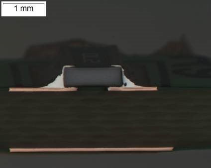
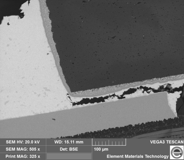
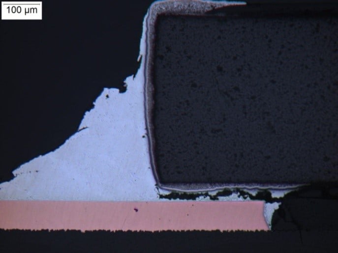
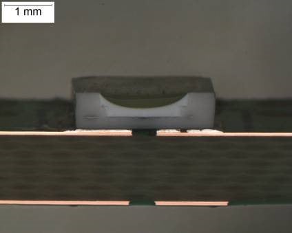
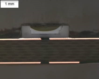
Following are a few examples of the assembled components that passed the thermal cycling test and the post-test visual inspection. When a cross-section examination was conducted, cracks were found in the solder joints. These are typical leadless surface mount chip resistors and LEDs. The chip resistor has a ceramic substrate and is end-terminated, and the LED is polymer-encapsulated and bottom-terminated, all reflowed with lead-free solder. All cracks were found between the bottom of the component and the PCB land. Some cracks shown in Figures 4 to 9 were obvious, whereas some hairline cracks were only revealed by high magnification examination under a microscope.
Conclusions
- Cross-sectional analysis reveals deleterious features in PCBs that cannot be discovered by non-destructive visual and x-ray inspection.
- Cross-sectional analysis reveals deleterious features in PCBs, even when they pass thermal cycling tests.
References
[1] Denis Kiesel, Radiography – Radioscopy …a technology comparison, 12th A-PCNDT 2006 – Asia-Pacific Conference on NDT, 5th – 10th Nov 2006, Auckland, New Zealand.
[2] P.E.J Flewitt and R.K.Wild, Physical Methods for Materials Characterisation, Second Edition, Institute of Physical Publishing, Bristol and Philadelphia, 2003.