Printed Circuit Board (PCB) Failure Analysis
Understand and rectify the root causes of PCB failure with industry-leading PCB failure analysis from the testing experts at Element. Looking for ways to optimize your printed circuit board designs while managing costs? We can help you identify and resolve critical issues before they impact production. Our expert team combines cutting-edge analysis techniques with deep industry knowledge to deliver actionable insights that enhance product quality and reduce failure rates – saving you time and money.
What is PCB Failure Analysis at Element?
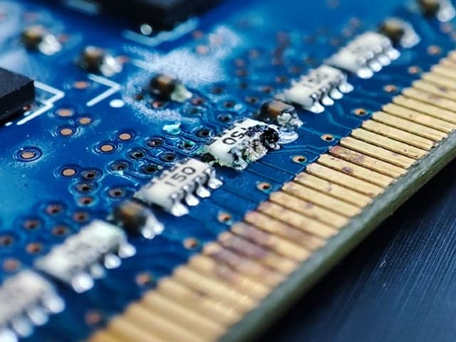
Printed Circuit Board (PCB) Failure Analysis is a systematic process used to identify the root cause of any PCB issues - ideally through analyzing symptoms before issues even begin - so you can take remedial action. At Element, we use a combination of detailed examination, industry-standard testing of PCBs, and expert analysis to help you understand and address any PCB failures. From component integration issues to material challenges, we enable you to make informed choices about design and fabrication faults and how to correct them, making sure that your PCB products meet both quality and cost requirements.
What can Element offer you for PCB Failure Analysis?

Key tests offered
Key tests offered
Element employs a systematic approach to PCB failure analysis, combining the following approaches, with each analysis tailored to your specific challenges and requirements:
- Micro-sectioning analysis to examine the internal structure of a PCB, providing crucial insights into potential defects and weaknesses.
- Solderability testing ensures that the solder joints are robust and reliable
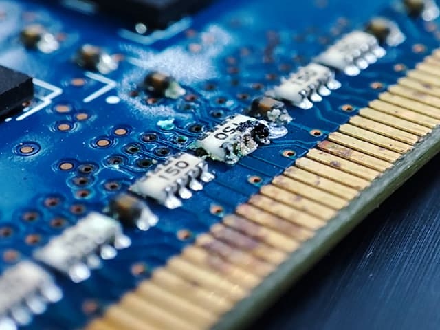
- PCB contamination testing helps identify any contaminants that may compromise the performance of the board.
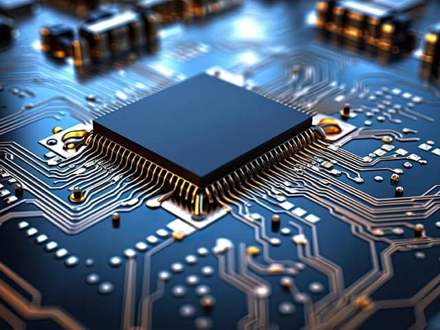
- Optical microscopy and scanning electron microscopy (SEM), helps perform detailed examinations of PCB surfaces and components, allowing us to uncover hidden flaws.
- X-ray inspection enables us to inspect the internal features of a PCB non-destructively, facilitating accurate failure analysis
- Conductive Anodic Filament (CAF) testing to check for current leakage, intermittent electrical shorts, and dielectric breakdown between conductors in PCBs.
Components and products we test
Components and products we test
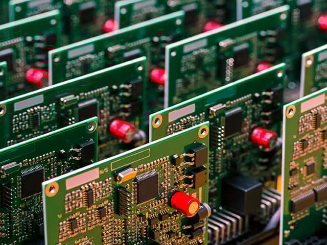
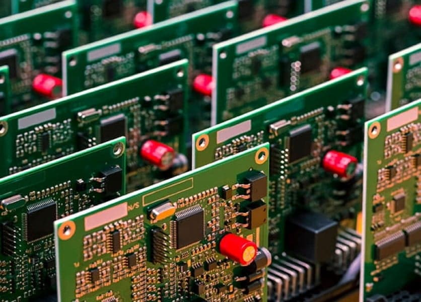
Our comprehensive testing capabilities cover everything from complete PCB assemblies to individual components. We specialize in analyzing high-speed printed circuit boards (HSCBs), solder joints, surface finishes, and copper plating. Our expertise extends to examining conductive anodic filament (CAF) issues and component integration challenges.
Cutting-edge equipment we use
Cutting-edge equipment we use
Our state-of-the-art facilities feature optical microscopy, scanning electron microscopy (SEM), and advanced X-ray inspection equipment. These technologies enable non-destructive examination of internal PCB features and detailed surface analysis for comprehensive failure investigation.
Which labs offer this service
Which labs offer this service
Notably among our circuit board testing labs, our Anaheim, CA and Baltimore, MD labs, formerly known as Microtek and Trace Labs, have more than 30 years of experience partnering with leading OEMs and manufacturers.
Components and materials we test
Your Challenges, Our Solutions
Complexity vs Cost Management
Component Integration in High-Speed PCBs
Lead-Free Assembly Risks
Surface Finish Selection
Element Experts at your service

Why Choose Element

Global Expertise Network
Comprehensive Solution Provider
Advanced Technical Capabilities
Customer-Focused Approach

Explore our global network of labs and find your nearest location
VIEW ALL LOCATIONSRelated services
Consumer Electronics Testing and Certification
Get expert consumer electronics testing to accelerate your market entry. Element's accredited EMC, safety & wireless compliance services facilitate smoother market entry.
Electrical Safety Testing and Certification Services
Accelerate your electrical product's journey to market with Element's comprehensive Electrical Safety Testing and Certification services. Navigate certification requirements efficiently, reducing time and costs while maintaining rigorous safety standards.
Printed Circuit Board (PCB) Testing
Looking for reliable printed circuit board testing? Element ensures PCB and assembly quality with advanced HATS2â„¢, counterfeit detection, and compliance. Learn More.
PCB Cleanliness & Contamination Testing
Ensure product reliability with Element's PCB Cleanliness & Contamination Testing. Our FTIR, IC, ROSE, and SEM/EDS analyses identify contaminants before they cause failures. Fast results from North America's PCB experts.
Conductive Anodic Filament (CAF) Testing
Conductive Anodic Filament (CAF) testing by Element ensures PCB reliability to IPC-TM-650. Prevent shorting failures, meet IPC standards and OEM specifications. Learn More.
Circuit Board Solder Testing
Trust Element's testing experts for easy, accurate solderability testing of your electronic components. Be confident that your solder joints are reliable and perform as expected, with our solder joint reliability testing and solder joint failure analysis.