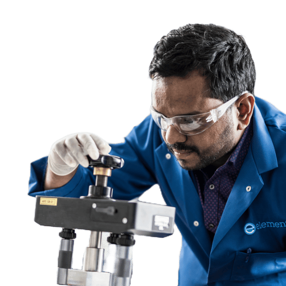
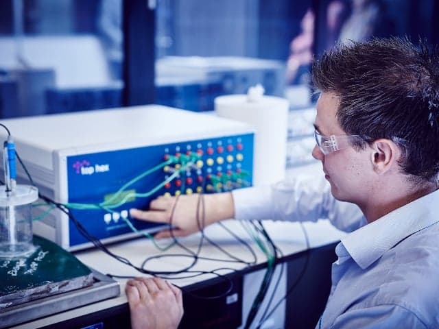
Surface Roughness Testing with 3D Optical Profilometry
Transform your component quality control with precise, non-contact surface roughness testing. Our advanced 3D optical profilometry delivers fast, accurate measurements for critical surface characteristics - from microscopic particles to wear patterns. Save time and resources while achieving optimal surface quality for your components.

What is Surface Roughness Testing with 3D Optical Profilometry at Element?
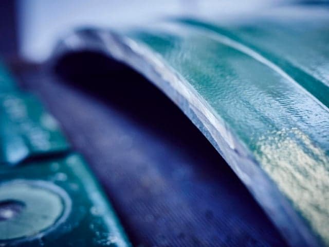
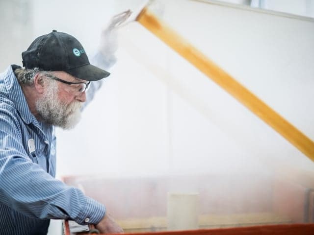
Surface roughness testing uses advanced optical technology to measure and analyze surface characteristics without contact. At Element, we provide comprehensive 3D optical profilometry services to evaluate surface smoothness, defects, and discontinuities - critical factors that impact component functionality, performance, and longevity.
What Can Element Offer You For Surface Roughness Testing?
Key tests offered
Key tests offered
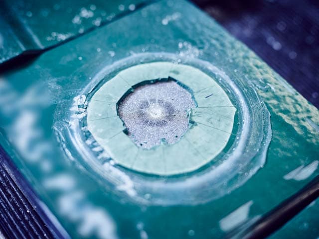
We provide comprehensive surface analysis including corrosion pit dimensioning, microscopic particle characterization, and wear pattern quantification. Our testing capabilities encompass:
- Surface roughness measurements
- Corrosion pit analysis
- Wear pattern visualization
- Coating depth assessment
- Thread dimension measurement
- Microscopic fractographic analysis
Components we test
Components we test
Our versatile testing capabilities cover virtually any solid material surfaces, from rough to smooth and hard to soft. We specialize in testing adhesive, deflectable, and challenging-to-measure components where traditional contact methods may not be suitable. Our expertise extends to:
- Precision-engineered components
- Threaded components
- Coated surfaces
- Flow-critical components
- Components requiring wear analysis
Methods and solutions offered
Methods and solutions offered
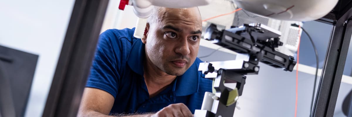
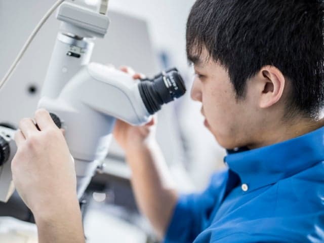
Using white light interferometry (WLI), we deliver non-contact surface metrology at microscopic scales. Our automated routines ensure consistent, reliable results while maintaining surface integrity throughout testing. We offer:
- Automated measurement routines
- Non-contact surface analysis
- White light interferometry
- Integrated optical microscopy
- Surface defect characterization
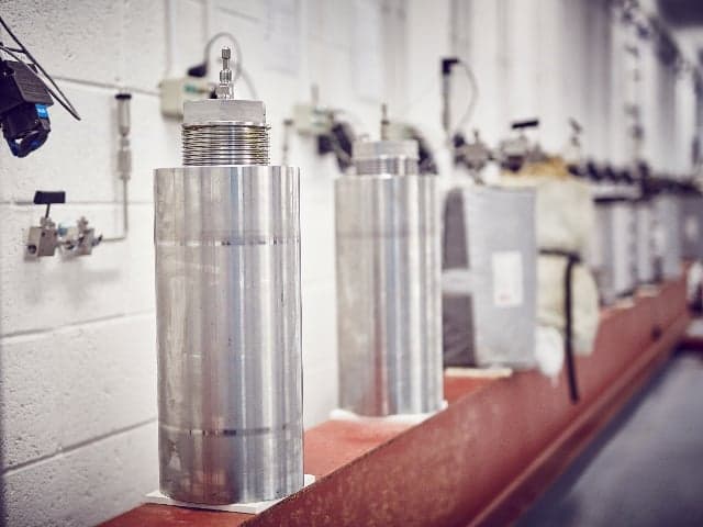
Cutting-edge equipment we use
Cutting-edge equipment we use
Our advanced white light interferometry optical profilometers feature integrated optical microscopes, enabling precise surface metrology at small scales. This technology allows for:
- Automated measurement capabilities
- High-precision surface analysis
- Non-contact measurements
- Integrated optical microscopy
- Comprehensive surface characterization
Advanced analysis capabilities
Advanced analysis capabilities
We complement our surface testing with additional metrology services, including:
- 3D metrology with industrial computed tomography
- 3D measuring services with photogrammetry
- Coordinate measuring machine inspection
- 3D scanning by laser tracking
- Comprehensive surface analysis solutions
Standards we test to and components we test
American Society of Mechanical Engineers
- ASME B46.1
International Standard Organisation
- ISO 4287:1997, ISO 25178-2:2012, ISO 13565:1996, ISO 12085:1996, ISO 4288:1996, ISO 25178-3:2012, ISO 3274:1996, ISO 11562:1996, ISO 16610 series, ISO25178-6:2010, ISO 12179:2000
High-precision components
- Threaded components (heights <10mm)>
- Flow-critical surfaces
- Precision-machined parts
- Components requiring wear analysis
Surface-critical components
- Coated components
- Components with roughness requirements
- Components requiring corrosion analysis
- Components needing defect characterization
Your Challenges, Our Solutions
Faster results that avoid component damage
Comprehensive defect prevention
Meeting Strict Quality and Regulatory Standards
Risk of Component Wear and Failure
Why Choose Element
Non-Destructive, High-Precision Testing
Expert Guidance & Industry Compliance
Advanced Automation & Speed
Seamless Integration with Other Metrology Services

Explore our global network of labs and find your nearest location
VIEW ALL LOCATIONSRelated services

Energy Coatings Testing Services
Protect your critical energy assets with Element's specialized coatings testing. We simulate extreme offshore and pipeline conditions to validate performance, prevent costly failures, and ensure compliance. Learn More.
Cathodic Disbondment Testing
Element's cathodic disbondment testing detects coating weaknesses before failure, simulating real-world conditions up to 204°C. Gain actionable insights to enhance protection for pipelines, offshore structures, and extreme environments.
Thermal Conductivity Testing Services
Element provides thermal conductivity testing and measurement services, including R-value, to ensure your materials insulate, conduct, and withstand temperature changes. Expert thermal conductivity testing for aerospace, oil & gas, and transportation materials. ISO/IEC 17025-accredited, non-destructive methods ensure safety, compliance, and performance in extreme conditions

IMO PSPC Coatings Testing of Seawater Ballast Tanks and Cargo Oil Tank
Element provides IMO PSPC coatings testing for seawater ballast and cargo oil tanks, simulating real-world conditions to verify compliance, prevent corrosion, and optimize coating performance.
Pipeline and Field Joint Coatings
Element provides expert pipeline and field joint coating testing to prevent corrosion, validate performance under extreme conditions, and support compliance with ISO 21809 standards for long-term infrastructure integrity.
Thermal Insulation Coating Testing
Element provides advanced thermal insulation coating testing for subsea pipelines, delivering precise data on durability, corrosion resistance, and compliance with industry standards to support material performance and longevity.
NORSOK M501 – Protective Coatings Testing for Offshore Applications
Element's NORSOK M501 coatings testing optimizes offshore protection, reducing maintenance and meeting compliance. Our experts provide third-party verification and guidance on Edition 7 requirements.
Surface and Coatings Testing Services
Optimize durability & compliance with Element’s Surface & Coatings Testing Services. Fast, accredited testing with expert insights to enhance product performance
Paint and Coating Testing Services
Get reliable paint & coating testing services to verify durability, ensure compliance, and reduce defects. Fast, integrated solutions tailored to your industry.
Coatings Chemical Resistance Testing
Protect your critical assets from chemical degradation with precise testing that simulates real-world exposure conditions. Our Coatings Chemical Resistance Testing identifies the most suitable solutions for your harsh operating environments, helping extend asset lifespans and prevent costly failures in oil and gas applications.
ISO 12944 Testing - Steel Corrosion Protection
Protect your steel structures from costly corrosion damage with Element's ISO 12944 testing services. Get expert testing across all corrosivity categories, ensuring compliance with international standards and long-term durability. Learn more.
Mechanical and Physical Testing of Coatings
Verify your coating performance, durability, compliance and damage resistance with Element's mechanical and physical testing. ISO/IEC 17025 certified testing for actionable insights. Learn More.
Water Immersion Testing
Element's water immersion testing evaluates coating performance in submerged conditions, identifying degradation risks like blistering and adhesion loss. Get reliable data to meet industry standards and enhance material longevity.

Peel Strength Testing
Our experts evaluate the bonding power and durability of adhesives through tests that simulate real-world peeling forces.
Positive Material Identification (PMI) Testing Services
Element's Positive Material Identification services provide a fast, cost-efficient method for determining the composition of metals and alloys, in the lab or in the field.
Residual Stress Measurement
Our experts offer a variety of techniques for residual stress measurement, including XRD and RSM, strain gaging, and Barkhausen Noise Analysis.
Coating and Paint Adhesion Testing
Adhesion testing services for paints and coatings to evaluate performance, meet ASTM standards, and address coating failures with expert analysis and actionable insights.
- Energy Coatings Testing Services
- Cathodic Disbondment Testing
- Thermal Conductivity Testing Services
- IMO PSPC Coatings Testing of Seawater Ballast Tanks and Cargo Oil Tank
- Pipeline and Field Joint Coatings
- Thermal Insulation Coating Testing
- NORSOK M501 – Protective Coatings Testing for Offshore Applications
- Surface and Coatings Testing Services
- Paint and Coating Testing Services
- Coatings Chemical Resistance Testing
- ISO 12944 Testing - Steel Corrosion Protection
- Mechanical and Physical Testing of Coatings
- Water Immersion Testing
- Peel Strength Testing
- Positive Material Identification (PMI) Testing Services
- Residual Stress Measurement
- Coating and Paint Adhesion Testing