Scanning Electron Microscopy in Failure Analysis

This article by Daniel Kiedrowski explains how Scanning Electron Microscopy (SEM) is used in failure analysis. It details how SEM, often paired with Energy Dispersive X-ray Spectroscopy (EDS), can reveal crack origins, surface features, contaminants and material inclusions at magnifications over 50,000x, helping engineers diagnose failures in both metallic and nonmetallic components.
What is SEM?
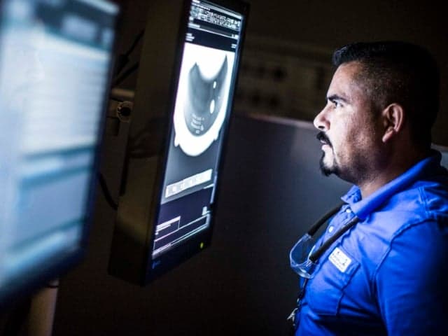
Scanning electron microscopy (SEM) is an invaluable tool in conducting failure analysis of metallic and non-metallic components and is used in some capacity in a large percentage of the investigations performed by Element. The SEM is a powerful tool in determining the origin(s), mode, and direction of propagation of cracks or fractures. SEM is used in conjunction with detailed documentation via macro photography and stereomicroscope to give a complete representation of the features or components being examined.
SEM is also employed heavily in the evaluation of debris, particles, residues, corrosion products, and other features requiring high magnification examination. The necessity and versatility of these instruments are evidenced by their presence in numerous Element laboratories company-wide.
How does SEM work?
An SEM operates by bombarding the surface of a sample with a focused beam of electrons. The electron beam excites the electrons of the material, resulting in the release of additional, secondary electrons. Alternatively, the electron beam can be backscattered by the sample and reemerge from the sample surface. Both secondary and backscattered electrons can be collected and displayed to provide an image of the surface being evaluated. The former provides greater resolution of surface features and the latter reveals greater topographic surface detail and information regarding the atomic weight of the surface being evaluated. Each type of electron plays a specific role in analyses via SEM depending on the objectives of the evaluation.
Is SEM right for you?
The chief advantage of an SEM in failure analysis is that the resulting image is generally similar to that of an optical photographic, but with significantly greater depth of field. SEM also allows examination at magnifications ranging from approximately 5X to greater than 50,000X, permitting documentation of large regions of a sample and microscopic features without changing instruments or lenses. The primary disadvantage of SEM is the lack of color imaging, which reinforces the importance of sample documentation via standard optical photography methods in conjunction with SEM. Examined samples must also be electrically conductive, although conductive surface coatings and the use of an SEM with a special variable pressure sample chamber and electron detectors mitigate many of these issues.
An extremely useful side effect of bombarding a surface with electrons is the generation of characteristic X-rays by the atoms of the material due to excitation by the electron beam. These X-rays can be detected and quantified by an energy-dispersive X-ray spectrometer (EDS) attached to the SEM. EDS provides the relative chemical composition of surfaces and features being examined using the SEM. This information can be extremely useful in the identification of corrosion products, surface residues or contaminants, material inclusions, wear debris and a host of other features that may not lend themselves to other conventional chemical analysis techniques. EDS results can also be combined with SEM images to form elemental EDS maps that provide a graphical representation of the distribution of elements in the surface or feature being examined.
To learn more about Scanning electron microscopy (SEM), or if you have any questions, contact our team today.
By Engaged Expert

Related Industries
Related Services
Failure Analysis Services
Need expert Failure Analysis Services? Identify root causes fast with Element's advanced testing, global reach, and rapid turnaround. Get expert insights today.

X-Ray Fluorescence (XRF) Testing Services
Element provides X-Ray Fluorescence (XRF) testing, available on-site or in the lab, for quick and precise chemical composition analysis of solids, liquids, and powders.

Scanning Electron Microscopy (SEM) with EDX Analysis
Scanning Electron Microscopy (SEM) and EDX analysis provide high-resolution imaging and elemental composition insights to detect surface defects, contaminants, and material properties, supporting manufacturers with detailed material evaluations.

Polymer Failure Analysis Services
Element's expert polymer failure analysis services investigate the cause of failure so you can take corrective action, limit damage, and prevent similar product failures in future.