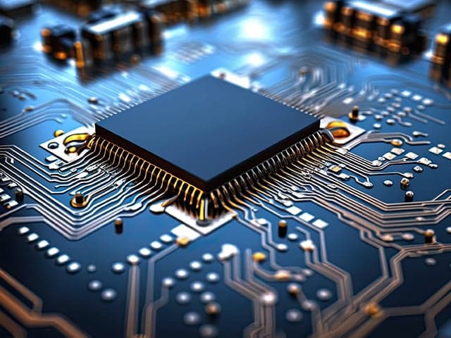
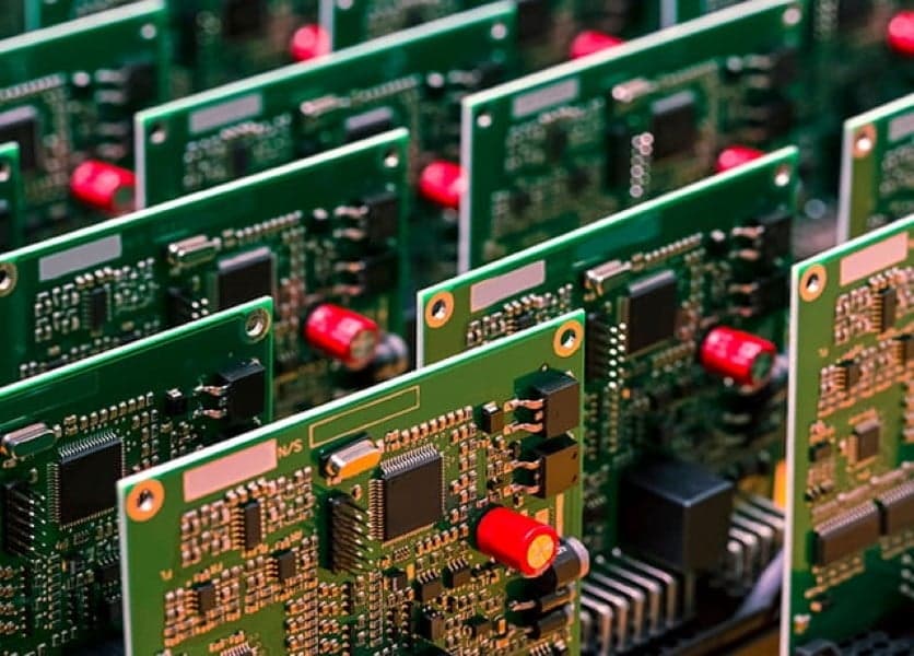
Printed Circuit Board (PCB) Testing
Element’s Printed Circuit Board Testing provides end-to-end testing solutions for PCBs, PCB assemblies and electronic components. Our state-of-the-art laboratories combine advanced technology like HATS2™ with expert analysis to help you prevent costly recalls, protect against counterfeits, and streamline your testing process. From early chip design to volume production, Element are the trusted partner for all your PCB testing needs, backed by 30+ years of expertise.
What is Printed Circuit Board (PCB) Testing at Element?
PCB testing is a manufacturing process to evaluate whether printed circuit boards and assemblies meet quality standards and are fit for purpose. At Element, we provide end-to-end testing solutions including expert analysis to validate components, ensure functionality, and perform failure analysis. We deliver comprehensive testing from raw materials through finished assemblies, helping you maintain quality while meeting industry standards and preventing costly recalls.
What can Element offer you for PCB Testing?
Components and materials we test
Components and materials we test
Support your entire PCB production cycle with comprehensive testing of raw materials, bare PCBs, and finished assemblies. Our expertise covers copper purity testing, laminate material qualification, conformal coating verification, and soldermask evaluation. We specialize in detecting counterfeit components through advanced inspection methods, protecting your supply chain integrity.
Key tests offered
Key tests offered
- Highly Accelerated Thermal Shock (HATS2™) Testing: A proprietary technology for faster, more reliable thermal shock testing.
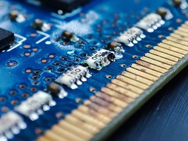
- Cross-Sectioning Analysis: Detects solder joint cracks, voids, lamination defects, poor wetting, land lift, and insufficient solder fill.
- Electrical Characterization: Detailed electrical performance evaluation.
- Microsection Analysis: Analysis as received, after thermal stress, thermal shock, or rework simulation.
- Root Cause Analysis: Comprehensive failure investigation to identify and resolve issues.
- Ball Shear Testing: Specialized technique for material integrity assessment.
- Wire Bond Pull Testing: Ensures bond reliability.
- Dynamic Mechanical Analysis (DMA): Material characterization under dynamic conditions.
- Thermal Analysis: Techniques such as DSC, TMA, TGA for evaluating thermal properties.
- Fourier Transform Infrared Spectroscopy (FTIR): Advanced material characterization method.
- Scanning Electron Microscopy with Energy-Dispersive X-Ray Spectroscopy (SEM/EDS): High-resolution material analysis.
- Consultancy Services: Expert support for failure analysis and performance optimization.
Methods and solutions offered
Methods and solutions offered
Visual Inspection
-
Mechanical Integrity
-
Solder Cracking
-
Burn Marks and Discoloration
-
Foreign Object Debris
-
Whisker Formation
-
Dendritic Growth
-
Flux Residue (IPC-A-610)
Material Quality and Conformance Testing
-
Raw Material Analysis: Evaluates PCB and PCA material properties.
-
Advanced Instrumentation: FTIR, SEM/EDS, Real-Time X-Ray.
-
Copper Testing: Purity, Tensile Strength, and Elongation.
-
Flammability Testing: IPC-4101 qualification for laminate materials.
-
Surface Insulation Resistance (SIR): Testing for material reliability.
-
Conductive Anodic Filament (CAF): Assessment of conductive pathways.
-
Electrochemical Migration (ECM): Evaluates potential for dendritic growth.
-
Thermal Analysis: Time to delamination, Coefficient of Thermal Expansion (CTE), Glass Transition Temperature (Tg / ΔTg).
-
Conformal Coating Tests: IPC-CC-830 or MIL-I-46058 compliance.
-
Soldermask Testing: IPC-SM-840 compliance.
Reliability and Performance Tests
-
Continuity Testing: Verification of electrical paths.
-
Dielectric Withstanding Voltage: Evaluates insulation strength.
-
Dimensional Inspection and Verification: Precision measurements for PCB conformance.
-
Flexural Endurance and Folding Flexibility: Durability under stress.
-
Ionic Cleanliness / Resistivity of Solvent Extract (ROSE): Contamination evaluation.
-
Moisture and Insulation Resistance (IR / MIR): Assessing resistance to environmental exposure.
-
Peel Strength: Adhesion quality of PCB layers.
-
Resistance to Solvents: Marking ink durability testing.
-
Solderability Testing (J-STD-003): Ensures solder wetting properties.
-
Thermal Cycling: Reliability testing under temperature variation.
-
Visual Examination: Per IPC-A-600 and IPC-A-610 standards.
Qualification and Conformance Testing
-
PCB qualification testing for new suppliers or manufacturing process changes.
-
Conformance testing schedules: Quarterly for Class 2, monthly for Class 3.
-
Acceptance testing: Conducted per lot.
-
Military specification testing: Performed on a three-year schedule.
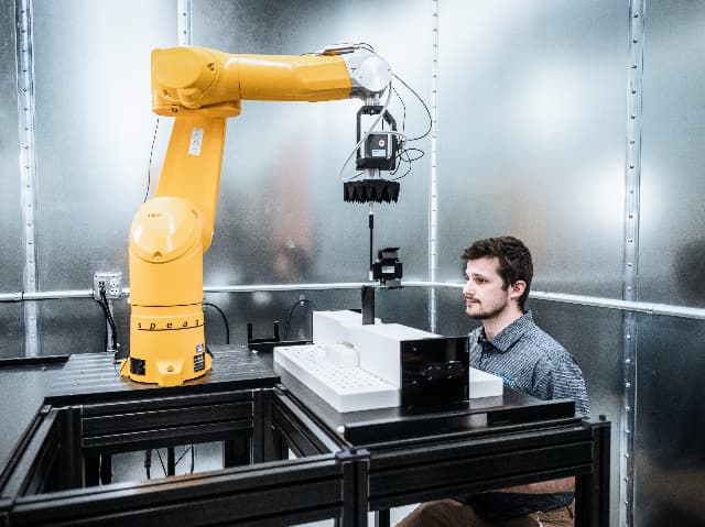
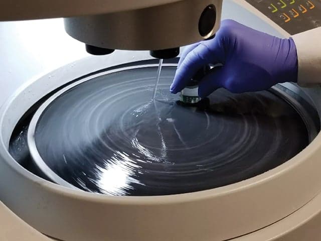
Cutting-edge equipment we use
Cutting-edge equipment we use
Utilize advanced instrumentation including FTIR, SEM/EDS, Real-Time X-Ray, and Scanning Acoustic Microscopy. Our HATS2™ technology provides superior thermal shock testing with continuous monitoring capabilities. Equipment includes high-speed precision resistance sampling networks and advanced cross-sectioning tools.
Which labs offer this service
Which labs offer this service
Notably among our circuit board testing labs worldwide, our Anaheim, CA and Baltimore, MD labs, formerly known as Microtek and Trace Labs, have more than 30 years of experience partnering with leading OEMs and manufacturers.
Standards we test to and materials we test
- Raw PCB materials
- Bare PCBs
- Finished PCAs
- Electronic components
- Copper materials
- Laminate materials
- Conformal coatings
- Soldermask
- Solder joints
- Plated-through holes
- Circuit board materials
- Component markings
- Packaging materials
- Circuit assemblies
Your Challenges, Our Solutions
Costly Product Failures
Counterfeit Component Threats
Time-Consuming Testing
Complex Compliance Requirements


Why Choose Element
Industry-Leading Experience
Comprehensive Testing Solutions
Advanced Technology Partner
Global Testing Network
30+Years Experience
2003Launch
7Global Regions
20+Testing Methods
Frequently asked questions
What types of PCB visual assessments do you perform?
We use IPC-A-610 to assess mechanical integrity, solder cracking, burn marks, discoloration, foreign object debris, whisker formation, dendritic growth, and flux residue on printed circuit boards.
What is HATS2™ testing?
HATS2™ (Highly Accelerated Thermal Shock) is a fast, reliable method for thermal shock testing. It uses extremely hot or cold air on stationary samples, enabling continuous resistance monitoring and precise detection of “glitch” conditions. Unlike traditional dual-chamber methods, HATS2™ reduces cycle time and eliminates costly sample transfers. In use since 2003, it supports in-situ convection reflow simulation and meets MIL-STD-202 Method 107 and IPC-TM-650 standards for thermal shock and reflow assembly simulations.
What is the difference between a PCB and a PCA?
The terms PCB (Printed Circuit Board) and PCA (Printed Circuit Assembly) refer to different stages in the lifecycle of circuit boards:
PCB is the bare board with conductive pathways, serving as the base for electronic components. A PCA is the assembled version of the PCB with all components installed, making it functional.
Summary of the Difference:
|
Aspect |
PCB |
PCA (PCBA) |
|
Definition |
Bare board with traces and vias. |
PCB with components assembled. |
|
Components |
No components. |
Includes all necessary components. |
|
Functionality |
Non-functional on its own. |
Fully functional when powered. |
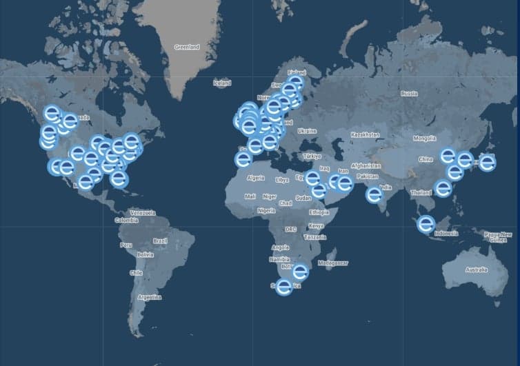
Explore our global network of labs and find your nearest location
VIEW ALL LOCATIONSRelated services

Conformal Coating & Inspection Testing
Element offers advanced conformal coating testing and PCB inspection to detect adhesion, electrical, and contamination issues, helping manufacturers meet industry standards and improve product reliability.
PCB Cross-Section (Microsection) Analysis
Ensure the integrity of your printed circuit boards with Element's expert PCB microsectioning & cross-section analysis. Precise results & industry-leading turnaround times.

Tin Whisker Testing
Element provides environmental testing or printed circuit boards (PCBs) to determine if your tin solder is likely to produce tin whiskers while in use.
Conductive Anodic Filament (CAF) Testing
Conductive Anodic Filament (CAF) testing by Element ensures PCB reliability to IPC-TM-650. Prevent shorting failures, meet IPC standards and OEM specifications. Learn More.

Electrochemical Migration (ECM) Testing
Element provides accredited EMC and EMI testing and certification services, helping businesses meet regulatory requirements, reduce costly redesigns, and bring products to market faster through expert compliance support.

Institute for Printed Circuits (IPC) Testing & Certification
Accelerate your product certification with Element's IPC testing services. Industry-leading expertise, comprehensive PCB testing, and flexible training options.
Ion Chromatography (IC) Testing for Electronics
Prevent electronic component failures with Element's precise ion chromatography testing. Get detailed ionic contamination analysis for printed circuit boards.

Surface Insulation Resistance (SIR) Testing
Measure the reliability of your printed circuit boards under real-world temperature and humidity conditions with surface insulation resistance (SIR) testing from Element.

Failure Analysis for Electronic Devices & Components Services
Element's comprehensive failure analysis services help you identify root causes, prevent future failures, and protect your brand reputation.
Circuit Board Solder Testing
Trust Element's testing experts for easy, accurate solderability testing of your electronic components. Be confident that your solder joints are reliable and perform as expected, with our solder joint reliability testing and solder joint failure analysis.
- Conformal Coating & Inspection Testing
- PCB Cross-Section (Microsection) Analysis
- Tin Whisker Testing
- Conductive Anodic Filament (CAF) Testing
- Electrochemical Migration (ECM) Testing
- Institute for Printed Circuits (IPC) Testing & Certification
- Ion Chromatography (IC) Testing for Electronics
- Surface Insulation Resistance (SIR) Testing
- Failure Analysis for Electronic Devices & Components Services
- Circuit Board Solder Testing