PCB Cross-Section (Microsection) Analysis
Ensure the integrity of your printed circuit boards with Element's expert PCB microsectioning and cross-section analysis services. Our IPC-certified technicians accurately analyze complex, multi-material PCBs including high-aspect ratio boards with features as small as 0.001". Whether for conformance testing, failure analysis, or vendor qualification, we deliver precise results with industry-leading turnaround times.
What is PCB microsectioning analysis at Element?
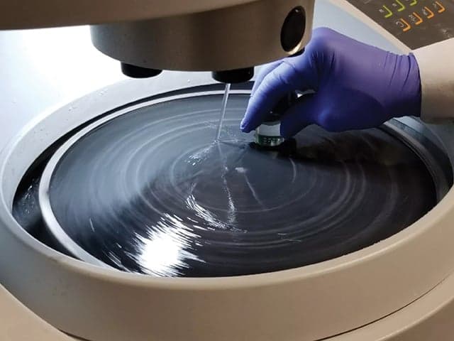
PCB microsectioning, also called cross-section analysis, is the most widely accepted method for analyzing the through-hole integrity of printed circuit boards (PCBs) or printed wiring boards (PWBs). At Element, we perform this delicate process with specialized expertise, ensuring precise cross-sectional preparation within 10% of the plated-through hole center. This precision is crucial when examining boards containing diverse materials with different hardness properties like glass, aramid fibers, copper, epoxy, and solder.
What can Element offer you for printed circuit board cross-section analysis?
Components We Test
Components We Test
Element offers comprehensive cross-section analysis for various board types and components, including multi-material PCBs containing glass, aramid fibers, kapton, copper, acrylic adhesive, epoxy, polyimide, Teflon, and solder. Our techniques account for the different relative hardness of these materials, ensuring accurate analysis regardless of material complexity.
Key Tests Offered
Key Tests Offered
Whether you require regular conformance cross-section analysis, failure analysis, vendor qualification, or lot verification, Element has the experience and knowledge to provide you with the highest quality testing and fastest turnaround available. Each test is performed with precision and according to industry standards to ensure your boards meet quality and reliability requirements.
Methods and Solutions Offered
Methods and Solutions Offered
We deliver precise cross-section analysis within 10% of the plated-through hole center, the critical area for accurate assessment. Our experts use specialized techniques to properly prepare and analyze samples despite the challenges presented by materials with different hardness properties and mounting media, ensuring reliable results for your quality control needs.
Which Labs Offer This Service
Which Labs Offer This Service
Notably among our circuit board testing labs worldwide, our Anaheim, CA and Baltimore, MD labs, formerly known as Microtek and Trace Labs, have more than 30 years of experience partnering with leading OEMs and manufacturers.
Training Services Available
Training Services Available
Beyond testing services, Element provides hands-on microsection preparation and analysis training for your in-house staff. This training can be conducted either at one of our laboratories or on-site at your facility, helping you improve the quality of your PCB microsections and build internal capabilities.
Standards we test to and products we test
All of Element's test inspection personnel for PCB analysis and PCBA analysis are certified to IPC-A-600 and IPC-A-610 visual acceptability standards.
- Printed Circuit Boards (PCBs)
- PCB Assemblies (PCBAs)
Your Challenges, Our Solutions
Complex Material Analysis
Specialized Expertise Required
High-Precision Analysis Needs
In-House Capability Building
Element Experts at your service

Why Choose Element
Historic Industry Experience
IPC-Certified Technicians
High-Aspect Ratio Capability
Fastest Turnaround Available
Frequently asked questions
What is ROSE testing and why is it important?
Resistivity of Solvent Extract (ROSE) Testing provides a quick quantification of overall PCB/assembly cleanliness. Using a simple resistivity meter, it delivers a singular value to rate cleanliness. ROSE testing is considered the workhorse of cleanliness testing due to its many advantages, including low cost and rapid assessment capabilities.
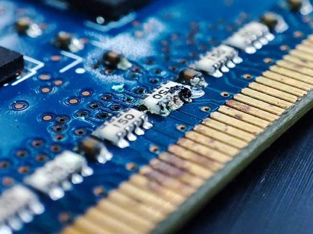
How do contaminants affect PCB performance?
Contaminants on PCBs can lead to corrosion, electrical shorts, high-resistance connections, and ultimately product failure. Ionic species and organic residues can particularly impact long-term reliability by causing gradual degradation of circuits and components over time.
When would you use FTIR versus SEM/EDS analysis?
FTIR spectroscopy is a non-destructive technique usually employed when a contaminant is believed to have an organic component, such as materials that could lead to corrosion resulting in high-resistance shorts. SEM/EDS analysis is typically paired with FTIR to investigate contaminants believed to have inorganic or metallic components, providing both visual and elemental information about an area of interest.
30 yearsof PCB testing experience
0.001"analysis of features with precision
10% marginaround plated-through hole
9,000+testing experts worldwide
Explore our global network of labs and find your nearest location
VIEW ALL LOCATIONSRelated services
Printed Circuit Board (PCB) Testing
Looking for reliable printed circuit board testing? Element ensures PCB and assembly quality with advanced HATS2â„¢, counterfeit detection, and compliance. Learn More.
Printed Circuit Board (PCB) Failure Analysis
Understand and rectify the root causes of PCB failure with industry-leading PCB failure analysis from the testing experts at Element. Optimize your PCB designs while managing costs. Learn More.

Institute for Printed Circuits (IPC) Testing & Certification
Accelerate your product certification with Element's IPC testing services. Industry-leading expertise, comprehensive PCB testing, and flexible training options.
Surface Insulation Resistance (SIR) Testing
Measure the reliability of your printed circuit boards under real-world temperature and humidity conditions with surface insulation resistance (SIR) testing from Element.